
At TPCA Show 2026, optical transceivers emerged as a major focus for the PCB industry. At the recently concluded OCP summit, NVIDIA and Cisco introduced the USFP design, targeting 400G per electrical lane. That puts the pressure in perspective: as optical transceivers get faster, what capabilities must the PCBs carrying their signals provide?

A Focus at TPCA Show: Optical Communications
At TPCA Show 2026 (2026/10/20–2026/10/22), the optical-communications initiatives of major PCB makers such as Zhen Ding and Unimicron made this trend tangible. In an interview at the show on 2026/10/20, Zhen Ding Chairman Shen Ching-fang described strong demand for high-speed optical communications and said the company expected its optical-module business to grow severalfold in 2027. The group is also expanding capacity for high-end products and accelerating its optical-transceiver efforts. Unimicron is repurposing existing factories to add optical-transceiver capacity, which its earlier investor briefing expected to begin coming online in 4Q26.
From Zhen Ding’s growth and expansion plans to Unimicron’s repurposing of existing factories, these leading manufacturers are putting resources into process upgrades and capacity. Their publicly disclosed mSAP specifications, investments and capacity plans are summarized in Exhibit 2 below.
So here’s my question: why does moving to 1.6T mean that optical-transceiver PCBs need mSAP too?
PCB Makers Step Up mSAP Investment as Optical Demand Grows
RMB 626 million in optical-module revenue in 1H26
Avary’s 1H26 optical-module revenue exceeded its full-year 2025 total of RMB 228 million. A new project plans 655,600 m² of annual capacity covering AI servers and high-speed optical modules. Zhen Ding targets severalfold growth in optical-module revenue; customers have booked 2027 capacity.
Potential monthly mSAP revenue scale of NT$2.5–3.0 billion in 2H27
Conditional on successful capacity expansion. Planned investment of NT$8–10 billion covers Chongqing, Luzhu and Dayuan.
Additional optical-module capacity expected in 4Q26
Existing facilities are being adapted to meet demand. A separately identifiable investment amount or capacity area for optical-module mSAP was not available in the material reviewed.
Planned annual capacity: 120,000 m²
The optical-module mSAP project involves approximately RMB 2.003 billion in total investment, using existing factory space in Zhuhai.
mSAP lines: 3 rising to a planned 5 by year-end
Three lines at the end of June 2026, four in August, and five planned by year-end. Boards for 800G and 1.6T optical modules have been delivered in volume.
October’s OCP Global Summit Raises the Bar for Optical Transceivers
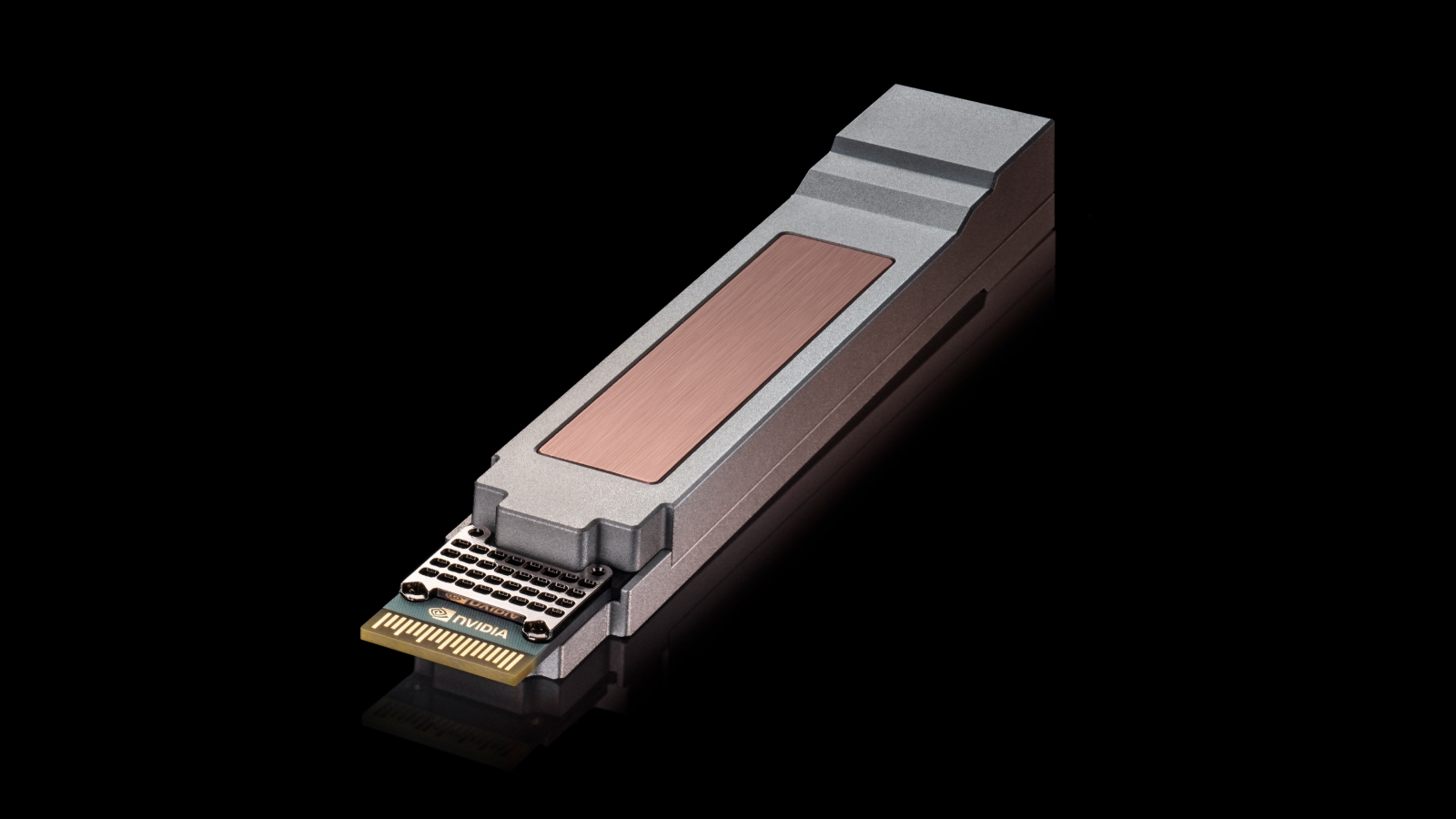
At the OCP Global Summit, which concluded in San Jose, California, on 2026/10/15, NVIDIA and Cisco jointly introduced the USFP design, offering 6.4T per module with an expansion path to 12.8T. From PCB makers building capabilities to data-center players advancing next-generation interfaces, optical-transceiver upgrades are progressing at both ends.
USFP’s 6.4T aggregate rate comes from 16 electrical lanes running at 400G each; expanding to 32 lanes brings the total to 12.8T. The key point is that each electrical lane must carry 400G. The traces carrying electrical signals inside the module must keep pace, making the high-speed demands on the PCB much more concrete.
Arista’s XPO, announced in March 2026, uses 64 electrical lanes at 200G each, delivering 12.8T per module. Exhibit 4 below brings together recently announced high-speed interconnect interfaces and module specifications, comparing electrical lane rates, aggregate rates and stages of development.
Electrical Lane Rates and Aggregate Rates of High-Speed Interconnects
16 × 400G = 6.4T → 32 × 400G = 12.8T
Announced: October 12, 2026 | Design initiative; lane-count expansion within the same architecture
64 × 200G = 12.8T
16 × 100G = 1.6T → 16 × 200G = 3.2T
Announced: June 2021 | Roadmap white paper: September 18, 2022
Why Does 1.6T Move to mSAP? Fine Traces and Trace Geometry Are Key
For 800G optical transceivers, HDI and mSAP still coexist in roughly equal proportions; at 1.6T and above, the shift is entirely toward mSAP. Why does a higher data rate require a different PCB process? Unimicron’s conference illustrations make the reasons concrete.
At the OCP APAC Summit in August 2026, Unimicron’s Jason Chen used process diagrams and trace cross sections to explain mSAP’s fine-line and geometry-control capabilities. Exhibit 5 reproduces the original slide: the process flow runs along the bottom, while the nearly rectangular copper cross section at the upper right highlights the relationship between vertical sidewalls and impedance consistency.
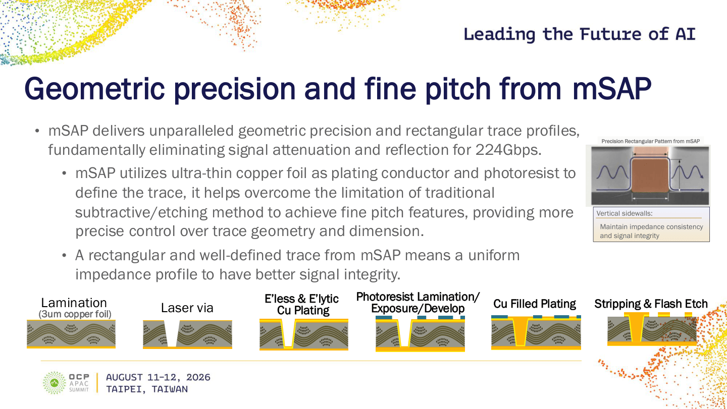
If you think a copper trace only needs to “make a connection,” high-speed transmission has news for you: even the shape of its sides needs attention. Traditional subtractive processing etches away unwanted copper, but etching also attacks the sides. You draw a nice, square profile, and the etched result makes you ask, “Hello, what happened here?” The cross section may be trapezoidal, and the width may deviate from the design. Unimicron’s flow starts with 3 μm copper foil, followed by laser drilling, copper plating, photoresist imaging and copper filling, then removal of the resist and excess thin copper. Defining the traces with photoresist and building them by electroplating enables tighter control over their shape and dimensions.
The cross section at the upper right shows how mSAP brings copper traces closer to their intended geometry. The sidewalls are nearly vertical, the cross section is nearly rectangular, and the edges are more clearly defined. Compared with the trapezoidal profiles and dimensional deviations associated with conventional etching, mSAP brings trace width, copper thickness and edges closer to the design values. This also makes it easier to maintain consistent impedance along the trace. Smaller impedance variations help reduce reflections as high-speed signals travel through it.
In the presentation, Unimicron explained that these well-defined, more uniform traces help reduce signal attenuation and reflections, particularly for electrical transmission at 224 Gb/s or above. The value of mSAP therefore goes beyond making traces finer: it also makes their geometry and dimensions more consistent, giving designers greater control over the paths that high-speed signals travel.
With Flip Chip, Low CTE Addresses Interconnect Reliability
Why do high-speed optical transceivers use flip chip? In its technical article on the design and manufacturing of 1.6T optical modules, USI writes: flip chip integrates digital signal processors (DSPs) and photonic integrated circuits (PICs) through high-density, short-distance interconnects, helping reduce parasitic effects and improve high-speed signal performance.
Chips expand when they get hot. Boards do too. The trouble is, you can’t just swell as much as you like—you also have to consider the one you’re connected to. CTE stands for coefficient of thermal expansion. In a flip-chip assembly, differences in expansion between the chip and the substrate beneath it can pull on the tiny interconnects. Appropriate low-CTE materials can help reduce expansion mismatch and interconnect stress.
High-Speed Optical Transceivers Demand Both Electrical Performance and PCB Reliability
Looking back at the investments discussed earlier, it becomes easier to see what capabilities PCB makers are adding. The 1.6T product generation has already brought mSAP into publicly disclosed process roadmaps, while plans for 400G electrical lanes continue to raise the demands on signal transmission and integration density.
mSAP provides tighter control over fine traces and their geometry. As high-speed interconnects increasingly adopt flip chip, differences in thermal expansion between materials also become a consideration for interconnect reliability.
As optical transceivers get faster, traces must preserve electrical performance in less space, and interconnects must remain reliable through temperature changes. Follow the story from optical modules to PCB processes, materials and packaging, and one thing becomes clear: part of the next step in optical communications starts with getting the copper right.
As Optical Communications Move to 1.6T, PCB Manufacturing Moves to mSAP

mSAP: Tighter Control of Fine Traces and Geometry
More consistent trace width, copper thickness and cross sections help bring high-speed signal paths closer to their design targets.
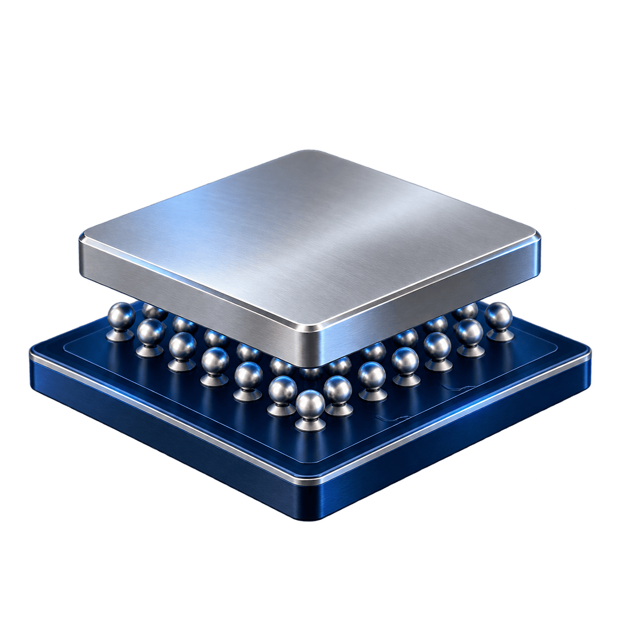
Low CTE: Interconnect Reliability Matters with Flip Chip
Appropriate low-CTE materials can help reduce thermal-expansion mismatch and interconnect stress.
Leave a Reply